UNSW has developed new dielectric patterning techniques to replace
photolithography. Less steps, less and cheaper chemicals for manufacturing high
efficiency solar cells.
The Technology
UNSW holds the world record for the efficiency of single junction silicon
solar cell. The record of 25.0% was achieved using photolithography, which is
too expensive for large scale commercial implementation.
The UNSW patterning techniques, which use inkjet printing or aerosol jet
printing, are cheaper than photolithography. They avoid the use of expensive
masks and mask aligners.
Digital images represent the etching patterns, so they are easily prepared
and changed. The etching pattern is printed to form openings in a dielectric
layer of silicon dioxide or PECVD silicon nitride.
The ‘resist’ technique typically etches grooves of 45 μm width, and holes ~40
μm in diameter. A single resist layer can be used for multiple patterning
processes.
How it works:
- A resist layer is formed over the dielectric surface.
- Patterned deposition of a plasticizer forms permeable regions
in the resist layer.
- Aqueous etchants then permeate through the patterned resist areas, and
etch openings in the dielectric layer.
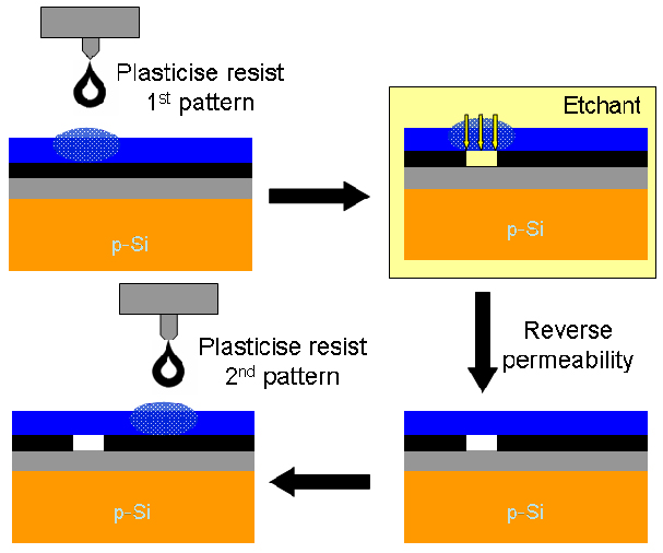
Process of patented ‘resist’ technique
The ‘direct’ technique, requires fewer steps and uses less and cheaper
chemicals than photolithography.
How it works:
1. An acidic polymer layer is formed over the dielectric surface.
2. A pattern of non-corrosive fluoride ions is deposited onto the
polymer
3. The fluoride ions react with the polymer to form
hydrogen fluoride (HF) locally, which then etches the underlying dielectric
layer.
Key Benefits
- Grooves narrow as 25 μm etched in a 75 nm thick PECVD silicon nitride
layer using an aerosol jet printer
- Immersion etching step is not needed so therefore largely reduced
quantities of toxic and corrosive etching fluid.
- Etched regions can be metal plated to form front metal contacts to the
solar cell.
- Significant OH&S advantages by reducing operator training expenses and
waste disposal issues.
- Other uses such as enhanced light capture into the cell by texturing the
silicon surface with dielectric masks created using UNSW’s dielectric
patterning techniques.
Opportunity
Collaborative partnership with UNSW to introduce production of high
efficiency solar cells for large scale commercial production.
More Information and Contact Details: PDF
verison of Non-Confidential Disclosure Document